

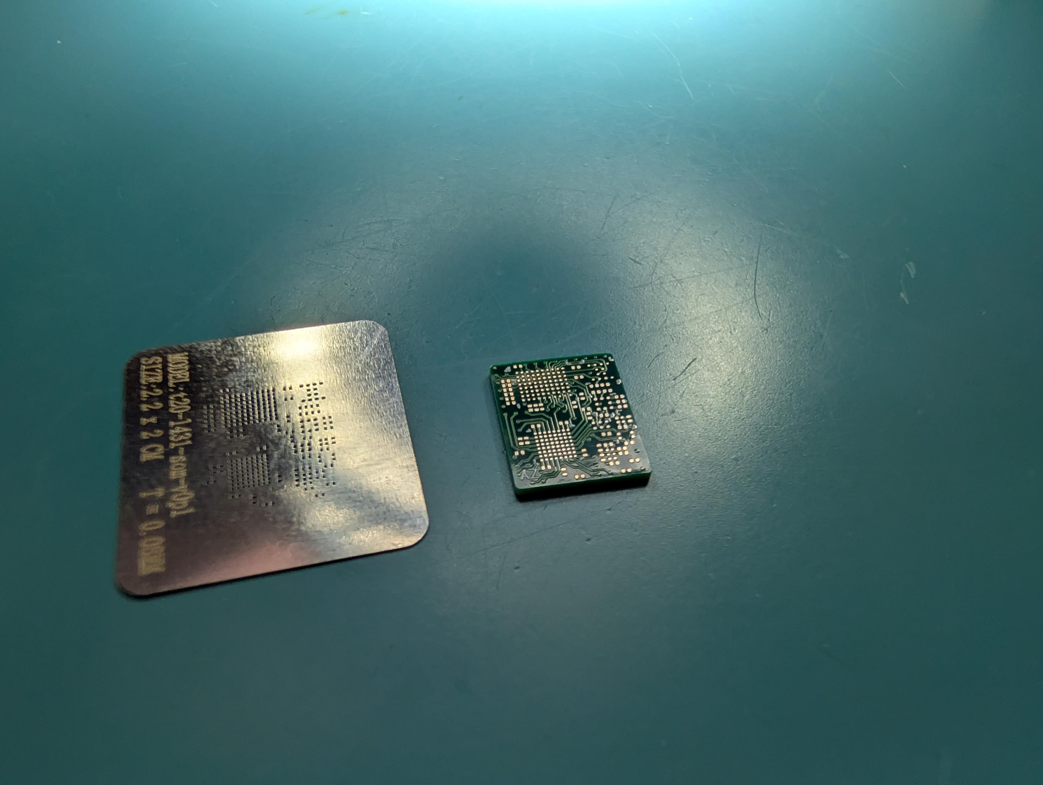
Hmmm. How do you get paste on a board this size....
0 Boosts
0 Likes
Obligatory banana for scale

This federated comment is not yet available here.
TI TPS22916BYFPR load switch.
Much more modern looking technology, several layers with a filler pattern that reminds me of TSMC but I have also seen from TI. The lack of TSMC corner fiducials make me think this is a TI in house fab.

On the home stretch! Here's the FPGA.
Efinix Trion T20 in the W80 package aka "Rebecca" for those of you doing bitstream RE.
Unlike every other WLCSP i can remember seeing, this one has a double layer RDL! You can see the die was originally designed for wire bonding and then fanned inward with two layers of copper and polyimide.
2 media files


(I have a much higher res version of this scan, not that you can see much besides power routing, and will be putting it on siliconprawn later. I also want to decap one of these in a normal wirebonded package and delayer it)
LP3986 dual LDO.
Has a National Semiconductor logo, looks to be made on a planarized three-metal process.
You can clearly see the two identical copies of the same base circuit, but the individual IP blocks are laid out a bit differently for some reason (it's not just two mirrors of the same layout).
The die is also made for wire bonding and there's visible probe scrub from wafer test.
And a ton of empty space. I wonder why they couldn't make the die a bit smaller?


Here's a first idea: double sided tape to bench, some extra boards around the one, usual kapton tape hinge design.
It's close enough I'm willing to paste it up and see how it goes