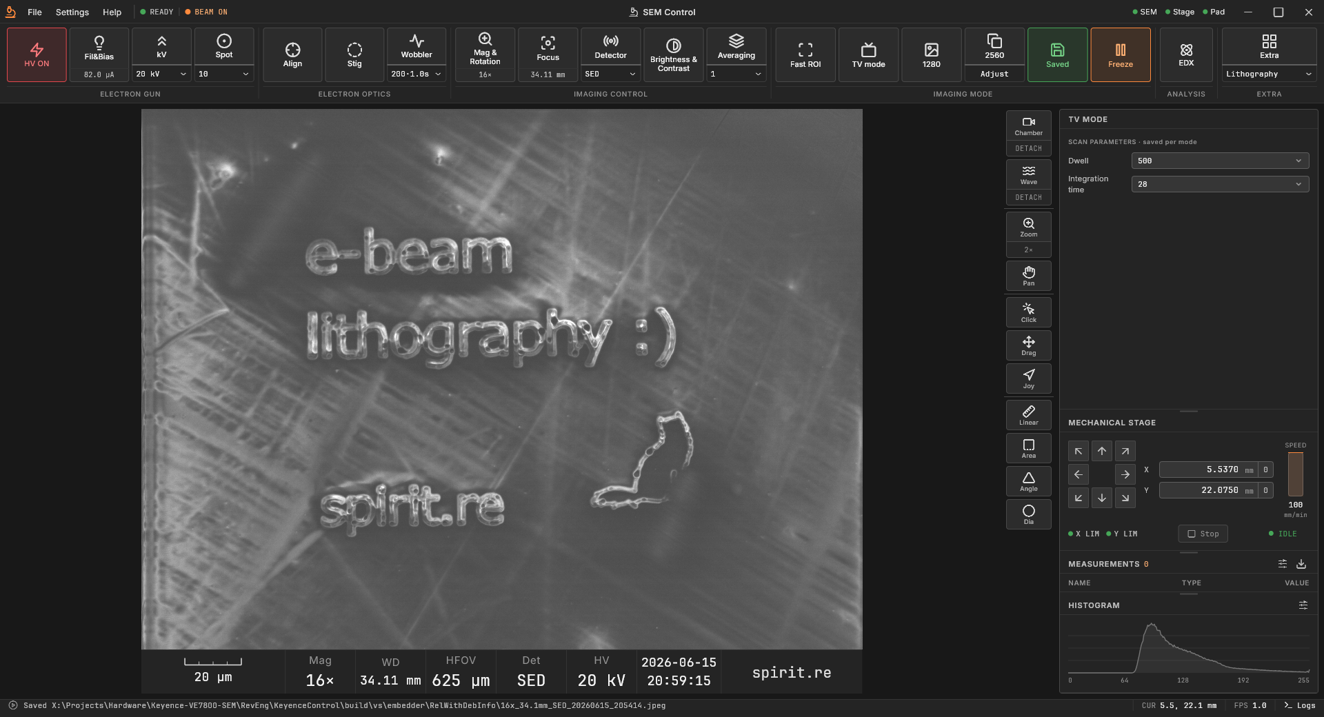
While working on my low-cost SEM project, I fully reverse-engineered the software that runs Keyence VE-series SEMs and integrated it into my new control suite, fixing big OEM bugs and *doubling* the image resolution, as well as adding e-beam lithography, stereo-3D, stacking & EDX
2 media files
0 Boosts
0 Likes
@jripley HF is for etch, not lithography. E-beam lithography is for patterning photoresist, which you then develop and process(etch, deposit, etc). But you *could* technically etch with a focused ion beam, just excruciatingly slowly. Definitely no desktop FIB though, not in the near future.
@spirit532 Yes, that's the idea—you wouldn't need HF because you just directly etch the surface instead. I've read various references to it being "slow" but I've never seen someone put a ballpark order of magnitude of how many zeroes "slow" is for, say, an IC being produced ~1980.
@jripley @spirit532 larger process node will be slower to process because you need to sweep a larger surface area
@spirit532 Wishing for the day where "Desktop SEM" is the big thing one year in the local Maker Faire, like "Desktop CNC" was this year 😊 Have been wondering if e-lithography could be used as a low-throughput replacement for the nastier parts of semiconductor production (remove the need for HF).